Arria 10 EMIF Simulation Guidance
Success! Subscription added.
Success! Subscription removed.
Sorry, you must verify to complete this action. Please click the verification link in your email. You may re-send via your profile.
- Intel Community
- Intel Community Knowledge Base
- Product Support Forums Knowledge Base
- FPGA Knowledge Base
- FPGA Wiki
- Arria 10 EMIF Simulation Guidance
Arria 10 EMIF Simulation Guidance
- Subscribe to RSS Feed
- Mark as New
- Mark as Read
- Bookmark
- Subscribe
- Printer Friendly Page
- Report Inappropriate Content
Arria 10 EMIF Simulation Guidance
9/92/Arria10_Simulation_Flow.jpg
Objective
This page explains how to extract the parameters to be entered in the 'Board Timing' tab of the Arria 10 External memory Interfaces GUI. This page also provides simulation guidance.
Note: Content on this page is applicable for DDR3, DDR4, RLDRAM3 and QDR IV, unless specifically mentioned otherwise.
Pre-layout simulation Guidance
Follow Altera layout guidelines for length and skew matching. Layout guidelines for various protocols can be found in the Volume 2 of the Altera EMIF handbook. Simulate your External memory interface related traces for the impedance. In some cases 40 ohm trace can work better than 50 ohm trace.
Once you have a preliminary layout, get an initial estimation off Board Timing parameters (board skews, setup/hold derating and ISI/Crosstalk parameters. Once you have initial estimation of ‘Board Timing parameters follow the flow mentioned in the next topic to get a sign off on the layout.
Detailed pre-layout simulation guidelines can be found here: DDR4_simulation_guidelines
Arria 10 Recommended Flow
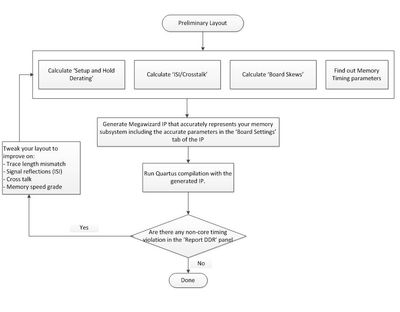
When you have the first draft of your memory interface layout, Altera recommends that you perform post-layout board-level simulation to calculate various Board Timing parameters. The later part of the section explains how to calculate the Channel Board Timing Parameters with a board simulation example. Once you obtain fairly accurate Board Timing numbers, enter these numbers in the Memory Interface IP. Generate the Memory Interface IP and run a Quartus compilation.
If you see non-core timing violations, then you need to change your layout accordingly to make improvements on trace length mismatch or ISI or crosstalk. Recalculate accurate ‘Channel Signal Integrity’, ‘Setup and Hold Derating’ and ‘Board Skew’ parameters. Regenerate and recompile the design. Repeat this step until you see positive timing margins.
System-level timing closure
External memory interface IP provided by Altera will close timing on the entire interface. This includes the PCB as well as DRAM. However, to get accurate sense of the timing, you need to provide accurate information about the DRAM and your PCB through ‘Memory Timing’ and ‘Board Timing’ tab. Accurate memory timing-related information can be obtained from memory datasheet. To get an accurate sense of ‘Board Timing’ you need to fill up the ‘Board Timing’ section in the Arria 10 external memory interface IP. The next section describes Altera’s guidance on providing information in the ‘Board Timing’ tab.
Note: Please do not use any simulation tool to perform system-level timing closure. Use simulation software to obtain channel loss and board skew data. Quartus will close the system level timing for you once you have entered accurate Memory Timing and Board timing information in the IP.
Filling out Board Timing
Board and Package Skews
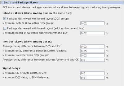
3/34/2_Board_Skews_Parameters.JPG
In this section you can input board length and length matching related information that represents your hardware through various parameters. The definitions of the these parameters are availaible in Vol 2 Chapter 9 of the EMIF Handbook. Alternatively, you can you Board Skew Parameter Tool to calculate these parameters. This tool is available on Altera web portal. You simply need to enter the board trace delays for all the relevant traces and the tool will output all the Board Skew parameters that you need to enter during IP generation process.
How to calculate trace delay?
Simple (not recommended): Measure the physical trace length (in mils or mm) in a layout tool. Convert the length of the trace to delay by using a lumped per inch number. For example, for FR4 material common practice is to use 150 ps/inch. This method of the calculating board skew is simple but not accurate hence we do not recommend it.
Advance (Recommended): Use a field solver on the stackup info to get the propagation velocity (ps/inch) for each leg of the trace (i.e. for each segment between layer changes). Multiply that by the physical length of each segment to get the propagation delay.
Slew Rates
If the rest of the parameters are calculated as per the guidance, slew rate information is redundant. Starting with 15.1, you will not see the Slew Rate section in the IP GUI. If you are using and older version of Quartus you can keep the slew rate to the default value.
Intersymbol Interference/Crosstalk
Channel Loss can be defined as shrinkage of available margins due to FPGA package and the PCB. These uncertainties (or Jitter) can be caused by FPGA, DRAM, and the PCB. Before we talk about how to calculate these uncertainties it is important that we understand we do we expect the customers to simulate.
There is three main cause of margins shrinkage:
1. ISI (Reflection)
2. Crosstralk (Induced voltage from nearby traces)
3. PDN (Loss of margin due to power supply design)
PDN affect (SSO and SSI) are taken into account internally by the timing analysis scripts.
For ISI and crosstalk effects we recommend that you perform a post-layout simulation on critical memory interface traces and obtain the following parameters.
Here is a short description on how to extract numbers from ISI/Cross talk simulation:
Address and command ISI/Crosstalk
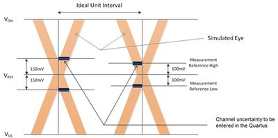
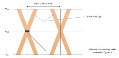
Simulate Address/Command/Control signals and capture eye at the DRAM pins. Use mem clock as a trigger of the Address/Command/Control signals of your memory interface. Measure the setup and hold side channel losses at the voltage thresholds mentioned in the memory vendor datasheet.
Number to be entered in the Quartus: Measured Loss on the Setup side + Measured Loss on the Hold side
The following figure illustrates this:
Write DQ ISI/Crosstalk
Simulate write DQ signals and capture eye at the DRAM pins. Use DQ Strobe (DQS) as a trigger of the DQ signals of your memory interface simulation. Measure the setup and hold side-channel losses at the VIH and VIL mention in the memory vendor datasheet.
Number to be entered in the Quartus: Measured Loss on the Setup side + Measured Loss on the Hold side
Vref = For center terminated I/O standards such as SSTL and HSTL, Vref is the midpoint of the supply voltage (e.g. 0.75 V for 1.5 V DDR3 with SSTL 15 I/O standard). For pseudo open drain (POD) type of I/O standard, memory IP performs calibration on Vref to adjust the Vref internally to the max possible eye-opening. Hence for POD type of I/O standard assume the Vref to be at the voltage level where you see maximum eye-opening in the simulated eye.
For example, the following figure illustrates this for DDR3 DQ signal:
Read DQ ISI/Crosstalk
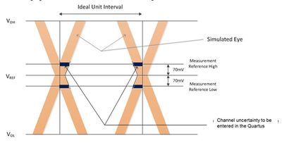
Simulate read DQ signals and capture eye at the FPGA die. Do not measure at pin you may see some unwanted reflection at the pin which might give you a false representation of eye opening at the input of the input buffer of the FPGA. Use DQ Strobe (DQS) as a trigger of the DQ signals of your memory interface simulation. Measure eye opening at +/- 70 mV with respect to Vref.
Number to be entered in the Quartus: (UI) - (Eye opening at +/- 70 mV with respect to Vref)
UI = Unit interval. For example if you are running your interface at 800 Mhz then effective data is 1600 Mbps give you the unit interval of 1/1600 = 625 ps.
Vref = For center terminated I/O standards such as SSTL and HSTL, Vref is the mid point of the supply voltage (e.g. 0.75 V for 1.5 V DDR3 with SSTL 15 I/O standard). For pseudo open drain (POD) type of I/O standard, memory IP performs calibration on Vref to adjust the Vref internally to the max possible eye opening. Hence for POD type of I/O standard assume the Vref to be at the voltage level where yuu see maximum eye opening in the simulated eye. For example,following figure illustrates this for DDR3 read DQ signal
Write/Read DQS ISI/Crosstalk
Simulate write/read DQS and capture eye. Measure the uncertainty at Vref.
FPGA IBIS file
Here is a link to the wiki page which describes how to generate IBIS file from Quartus. It also describes the modification that you need to do to the IBIS file so you are following the above-mentioned guidelines.
Hyperlynx DDR Wizard
You can choose the tool of your liking to perform simulation and extract out the ‘Intersymbol Interference/Crosstalk’ based on the recommendation given above. Hyperlynx’s DDR Wizard is one such tool that we believe is easy to use once you have a preliminary layout available. DDR Wizard gives you an easy to use interface to run the simulation on the entire memory interface at the same time.
Please note that we do not recommend that you use DDR Wizard for the purposes of timing closure. We recommend that you use DDR Wizard to extract the ‘Intersymbol Interference/Crosstalk’ and rely upon Quartus for the Interface level timing closure.
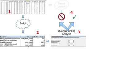
Here is a short summary of using DDR Wizard to perform system-level timing closure along with Quartus:
1. Follow the steps provided in the lab (see below) to simulate the memory interface. The sections below provide you with a way to simulate DDR3 and DDR4 with DDR Wizard. As a result of the Batchwizard simulation, you will get a bunch of .csv files for different data groups.
2. Run the Excel script provided by Altera with the result files generated by DDR Wizard as inputs. The script will spit out the ‘Intersymbol Interference/Crosstalk’ numbers to be entered in the Quartus. Excel script is available at this link as one of the attached zip file (Channel Loss Calculation Tool)
3. Run Quartus timing analysis and make sure you don’t see any non-core timing violation.
4. If you see a non-core timing violation tweak your layout accordingly and repeat steps 1, 2 and 3 until you see timing passing.
DDR3 Virtual Lab
Altera has worked with Mentor to create a DDR3 lab that shows you how you can set up DDR Wizard for the purpose of extracting out ‘Intersymbol Interference/Crosstalk’ numbers. Here is the link to that lab. All you need to do is create a user ID and get started with DDR Wizard lab. You don’t need any Hyperlynx license to work with the lab.
http://www.mentor.com/pcb/product-eval/hyperlynx-ddr-wizard
DDR4 Lab
If you have Hyperlynx Simulation Software installed on your computer, you can download the DDR4 lab project files and follow the instructions in the step by step guide to simulate a PCB with Arria 10 FPGA with DDR4 DRAM module. It will also walk you through on how to extract the 'Channel ISI/Crosstalk' numbers from Batchwizard results.
Note: You will need Hyperlynx Boardsim v9.2 or above in order to be able to simulate DDR4.
Step by step instructions on how to run the DDR4 lab.
Community support is provided during standard business hours (Monday to Friday 7AM - 5PM PST). Other contact methods are available here.
Intel does not verify all solutions, including but not limited to any file transfers that may appear in this community. Accordingly, Intel disclaims all express and implied warranties, including without limitation, the implied warranties of merchantability, fitness for a particular purpose, and non-infringement, as well as any warranty arising from course of performance, course of dealing, or usage in trade.
For more complete information about compiler optimizations, see our Optimization Notice.
